Two MIT teams selected for NSF sustainable materials grants
Chosen from 16 finalist teams, the MIT-led projects will investigate quantum topological materials and sustainable microchip production.

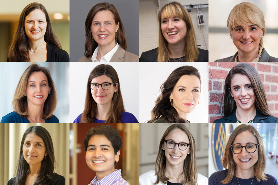
Two teams led by MIT researchers were selected in December 2023 by the U.S. National Science Foundation (NSF) Convergence Accelerator, a part of the TIP Directorate, to receive awards of $5 million each over three years, to pursue research aimed at helping to bring cutting-edge new sustainable materials and processes from the lab into practical, full-scale industrial production. The selection was made after 16 teams from around the country were chosen last year for one-year grants to develop detailed plans for further research aimed at solving problems of sustainability and scalability for advanced electronic products.
Of the two MIT-led teams chosen for this current round of funding, one team, Topological Electric, is led by Mingda Li, an associate professor in the Department of Nuclear Science and Engineering. This team will be finding pathways to scale up sustainable topological materials, which have the potential to revolutionize next-generation microelectronics by showing superior electronic performance, such as dissipationless states or high-frequency response. The other team, led by Anuradha Agarwal, a principal research scientist at MIT’s Materials Research Laboratory, will be focusing on developing new materials, devices, and manufacturing processes for microchips that minimize energy consumption using electronic-photonic integration, and that detect and avoid the toxic or scarce materials used in today’s production methods.
Scaling the use of topological materials
Li explains that some materials based on quantum effects have achieved successful transitions from lab curiosities to successful mass production, such as blue-light LEDs, and giant magnetorestance (GMR) devices used for magnetic data storage. But he says there are a variety of equally promising materials that have shown promise but have yet to make it into real-world applications.
“What we really wanted to achieve is to bring newer-generation quantum materials into technology and mass production, for the benefit of broader society,” he says. In particular, he says, “topological materials are really promising to do many different things.”
Topological materials are ones whose electronic properties are fundamentally protected against disturbance. For example, Li points to the fact that just in the last two years, it has been shown that some topological materials are even better electrical conductors than copper, which are typically used for the wires interconnecting electronic components. But unlike the blue-light LEDs or the GMR devices, which have been widely produced and deployed, when it comes to topological materials, “there’s no company, no startup, there’s really no business out there,” adds Tomas Palacios, the Clarence J. Lebel Professor in Electrical Engineering at MIT and co-principal investigator on Li’s team. Part of the reason is that many versions of such materials are studied “with a focus on fundamental exotic physical properties with little or no consideration on the sustainability aspects,” says Liang Fu, an MIT professor of physics and also a co-PI. Their team will be looking for alternative formulations that are more amenable to mass production.
One possible application of these topological materials is for detecting terahertz radiation, explains Keith Nelson, an MIT professor of chemistry and co-PI. This extremely high-frequency electronics can carry far more information than conventional radio or microwaves, but at present there are no mature electronic devices available that are scalable at this frequency range. “There’s a whole range of possibilities for topological materials” that could work at these frequencies, he says. In addition, he says, “we hope to demonstrate an entire prototype system like this in a single, very compact solid-state platform.”
Li says that among the many possible applications of topological devices for microelectronics devices of various kinds, “we don’t know which, exactly, will end up as a product, or will reach real industrial scaleup. That’s why this opportunity from NSF is like a bridge, which is precious, to allow us to dig deeper to unleash the true potential.”
In addition to Li, Palacios, Fu, and Nelson, the Topological Electric team includes Qiong Ma, assistant professor of physics in Boston College; Farnaz Niroui, assistant professor of electrical engineering and computer science at MIT; Susanne Stemmer, professor of materials at the University of California at Santa Barbara; Judy Cha, professor of materials science and engineering at Cornell University; industrial partners including IBM, Analog Devices, and Raytheon; and professional consultants. “We are taking this opportunity seriously,” Li says. “We really want to see if the topological materials are as good as we show in the lab when being scaled up, and how far we can push to broadly industrialize them.”
Toward sustainable microchip production and use
The microchips behind everything from smartphones to medical imaging are associated with a significant percentage of greenhouse gas emissions today, and every year the world produces more than 50 million metric tons of electronic waste, the equivalent of about 5,000 Eiffel Towers. Further, the data centers necessary for complex computations and huge amount of data transfer — think AI and on-demand video — are growing and will require 10 percent of the world’s electricity by 2030.
“The current microchip manufacturing supply chain, which includes production, distribution, and use, is neither scalable nor sustainable, and cannot continue. We must innovate our way out of this crisis,” says Agarwal.
The name of Agarwal’s team, FUTUR-IC, is a reference to the future of the integrated circuits, or chips, through a global alliance for sustainable microchip manufacturing. Says Agarwal, “We bring together stakeholders from industry, academia, and government to co-optimize across three dimensions: technology, ecology, and workforce. These were identified as key interrelated areas by some 140 stakeholders. With FUTUR-IC we aim to cut waste and CO2-equivalent emissions associated with electronics by 50 percent every 10 years.”
The market for microelectronics in the next decade is predicted to be on the order of a trillion dollars, but most of the manufacturing for the industry occurs only in limited geographical pockets around the world. FUTUR-IC aims to diversify and strengthen the supply chain for manufacturing and packaging of electronics. The alliance has 26 collaborators and is growing. Current external collaborators include the International Electronics Manufacturing Initiative (iNEMI), Tyndall National Institute, SEMI, Hewlett Packard Enterprise, Intel, and the Rochester Institute of Technology.
Agarwal leads FUTUR-IC in close collaboration with others, including, from MIT, Lionel Kimerling, the Thomas Lord Professor of Materials Science and Engineering; Elsa Olivetti, the Jerry McAfee Professor in Engineering; Randolph Kirchain, principal research scientist in the Materials Research Laboratory; and Greg Norris, director of MIT’s Sustainability and Health Initiative for NetPositive Enterprise (SHINE). All are affiliated with the Materials Research Laboratory. They are joined by Samuel Serna, an MIT visiting professor and assistant professor of physics at Bridgewater State University. Other key personnel include Sajan Saini, education director for the Initiative for Knowledge and Innovation in Manufacturing in MIT’s Department of Materials Science and Engineering; Peter O’Brien, a professor from Tyndall National Institute; and Shekhar Chandrashekhar, CEO of iNEMI.
“We expect the integration of electronics and photonics to revolutionize microchip manufacturing, enhancing efficiency, reducing energy consumption, and paving the way for unprecedented advancements in computing speed and data-processing capabilities,” says Serna, who is the co-lead on the project’s technology “vector.”
Common metrics for these efforts are needed, says Norris, co-lead for the ecology vector, adding, “The microchip industry must have transparent and open Life Cycle Assessment (LCA) models and data, which are being developed by FUTUR-IC.” This is especially important given that microelectronics production transcends industries. “Given the scale and scope of microelectronics, it is critical for the industry to lead in the transition to sustainable manufacture and use,” says Kirchain, another co-lead and the co-director of the Concrete Sustainability Hub at MIT. To bring about this cross-fertilization, co-lead Olivetti, also co-director of the MIT Climate and Sustainability Consortium (MCSC), will collaborate with FUTUR-IC to enhance the benefits from microchip recycling, leveraging the learning across industries.
Saini, the co-lead for the workforce vector, stresses the need for agility. “With a workforce that adapts to a practice of continuous upskilling, we can help increase the robustness of the chip-manufacturing supply chain, and validate a new design for a sustainability curriculum,” he says.
“We have become accustomed to the benefits forged by the exponential growth of microelectronic technology performance and market size,” says Kimerling, who is also director of MIT’s Materials Research Laboratory and co-director of the MIT Microphotonics Center. “The ecological impact of this growth in terms of materials use, energy consumption and end-of-life disposal has begun to push back against this progress. We believe that concurrently engineered solutions for these three dimensions will build a common learning curve to power the next 40 years of progress in the semiconductor industry.”
The MIT teams are two of six that received awards addressing sustainable materials for global challenges through phase two of the NSF Convergence Accelerator program. Launched in 2019, the program targets solutions to especially compelling challenges at an accelerated pace by incorporating a multidisciplinary research approach.
What's Your Reaction?


